.jpg)
Trust is earned when actions meet promises. Abiding by this belief, we at Sunstream provide quality service in short turnaround time to customers across the globe. Appreciated for reducing operational and development cost substantially, our simplified project management processes ensures maximum output and outcomes.
Flexible and available round the clock, a team of experts are deployed at the service of your business to ensure that expectations are not just met but surpassed.
All that would take to love and trust us is, a single phone call.Give it a shot – that’s our first promise!

SunStream Global Technologies specializes in Electronic Design, Mechanical Design, Product Development, and IT services. We help OEMs enhance efficiency through tailored solutions, including Sustenance Engineering, Re-Engineering, Product Environmental Compliance, and Engineering Process Outsourcing.
With a global delivery model, we optimize development costs while fostering trust and long-term partnerships. Our strong alliances with leading product companies enable us to deliver customized solutions in Electronic Design, Mechanical Design, Compliance, and Data Management.
Customer focus and commitment drive our success, with passion and expertise at the core of our team.

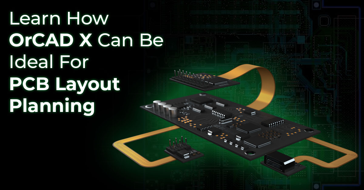
SunStream Engineering specializes in plant engineering, product development, and environmental compliance services, offering expertise in process engineering, design, embedded software, PCB design, and regulatory adherence.

Introduction
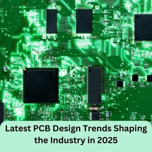
Printed Circuit Board (PCB) design is continuously evolving with advancements in technology. In 2025, innovations in PCB design services are transforming the way electronic circuits are developed and optimized. With an increasing demand for high-performance and compact designs, engineers are integrating new strategies to enhance PCB layout services. This article explores the latest trends in PCB design and how they are shaping the industry in 2025.
1. High-Density Interconnect (HDI) PCBs - High-Density Interconnect (HDI) technology is becoming the preferred choice for modern electronics due to its ability to enhance signal integrity and reduce board size. By utilizing micro vias, blind vias, and buried vias, HDI PCBs offer higher wiring density, improving overall performance.
2. Miniaturization and Compact Designs - With the growing demand for wearable devices, IoT applications, and compact electronic gadgets, PCB layout services are focusing on reducing board size while maintaining efficiency. The trend of miniaturization requires precise routing techniques and the use of flexible PCBs.
3. Flexible and Rigid-Flex PCBs - The demand for flexible PCBs has increased, allowing designers to create more durable and versatile electronic products. Rigid-flex PCBs combine the benefits of rigid and flexible circuits, offering superior reliability for applications in medical, aerospace, and consumer electronics.
4. Advanced PCB Materials - New PCB materials, such as high-frequency laminates and metal-core substrates, are gaining popularity. These materials enhance thermal management and signal transmission, making them suitable for high-speed applications and power electronics.
5. Multi-Layer PCB Advancements - As electronic components become more complex, multi-layer PCBs are playing a crucial role in improving circuit density and performance. Engineers are now using advanced stacking techniques to optimize signal flow and reduce electromagnetic interference.
6. Integration of AI and Automation - Artificial Intelligence (AI) and automation are revolutionizing PCB design services. AI-powered software tools assist in optimizing layouts, reducing design errors, and predicting potential circuit issues before fabrication. Automation also accelerates the design-to-production process, enhancing efficiency.
7. Thermal Management Innovations - Efficient heat dissipation is a critical aspect of PCB layout services. Advanced cooling techniques, such as embedded heat sinks and thermal vias, help prevent overheating in high-power applications. Designers are incorporating better thermal simulation tools to enhance PCB reliability.
8. 3D Printing in PCB Manufacturing - 3D printing technology is gradually making its way into PCB manufacturing. This innovative approach enables rapid prototyping and customization of PCB designs. With additive manufacturing, designers can experiment with complex structures without the limitations of traditional fabrication methods.
9. Internet of Things (IoT) and Smart PCB Integration - The rise of IoT devices has led to the development of smart PCBs that support wireless communication, sensors, and real-time data processing. PCB designers are integrating IoT connectivity features to enhance automation and remote control capabilities.
10. Sustainable and Eco-Friendly PCB Design - Environmental concerns are pushing the industry towards sustainable PCB manufacturing. The use of lead-free soldering, biodegradable materials, and energy-efficient production processes is gaining traction. Green PCB initiatives are aligning with global regulations to reduce electronic waste.
11. Enhanced Security Measures in PCB Design - With the increasing risk of cyber threats, PCB design services are incorporating security features such as hardware encryption and secure boot mechanisms. These measures help protect sensitive data and prevent unauthorized access to electronic devices.
12. High-Speed and High-Frequency PCB Design -
The demand for high-speed data transmission in telecommunications and computing industries is driving advancements in high-frequency PCB design. Low-loss materials, controlled impedance routing, and advanced signal integrity techniques are crucial for maintaining performance.
13. Improved Design Verification and Testing - Design verification and testing are becoming more sophisticated with simulation software and automated testing tools. Engineers are leveraging advanced verification techniques to detect potential flaws and ensure PCB functionality before production.
14. Wireless Charging and Power Management - Wireless charging technology is influencing PCB layout services by integrating efficient power transfer circuits. Improved power management solutions help extend battery life and enhance energy efficiency in portable electronics.
15. Future of PCB Prototyping - The future of PCB prototyping involves a combination of AI-driven design, 3D printing, and cloud-based collaboration. Engineers can now iterate faster, reducing development time and costs while maintaining precision and reliability.
Conclusion
The PCB design industry is undergoing significant transformations in 2025, driven by miniaturization, AI integration, advanced materials, and sustainable manufacturing. PCB design services are evolving to meet the increasing demand for high-performance and energy-efficient electronic solutions. As technology progresses, staying updated with these trends is essential for engineers, manufacturers, and businesses looking to optimize their PCB development processes.

.jpg)
.jpg)
.jpg)